


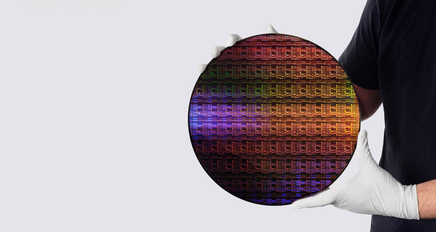

IBM this week claimed the first sub-nanometre chip, a generation it calls the 0.7nm, or 7-angstrom, node. It says the design packs nearly 100 billion transistors onto a fingernail-sized surface, about twice the density of its 2nm chip from 2021, with up to 50% more performance or 70% better energy efficiency. Production could begin within five years.
“This is an important engineering milestone,” said Francesco Petruccione, director of the National Institute for Theoretical and Computational Sciences (NITheCS) and professor of quantum computing at Stellenbosch University. “It shows that chip manufacturers are still finding ways to make computer chips more powerful and more energy-efficient, despite many experts believing that traditional scaling was approaching its limits.”
For decades, chips improved by shrinking transistors and packing more side by side on a flat sheet of silicon. That approach is hitting the limits of physics. IBM’s answer, a design it calls “nanostack”, stacks transistors on top of one another, like flats in a tower block rather than houses spread across open veld, so the same footprint can now hold far more.
IBM has described the redesign, not the shrinking, as the real story. “We’re not just making smaller transistors; we’re reinventing how chips are built,” said IBM Research director Jay Gambetta.
Petruccione agreed that is the crux: “The real innovation is not simply making transistors smaller, but redesigning how they are arranged in three dimensions, opening a new path for future generations of computing hardware.” Labels like “2nm” and “0.7nm” are names for a generation of technology, not the literal width of a transistor.
For scale, today’s best laptop processor, Apple’s M3 Max, has about 92 billion transistors across the whole chip; IBM fits a comparable number onto a single fingernail. Chip makers spend such a gain on more speed or lower power, and Petruccione expects both to reach users.
The impact
“For consumers, it could eventually translate into faster smartphones and laptops, longer battery life and more capable AI assistants running directly on devices,” he said. “For businesses, the bigger impact is likely to be lower energy costs in data centres and the ability to process much larger AI workloads, making advanced AI applications more affordable and widely available.”

Better chips go to the heart of the AI boom. “AI progress increasingly depends not only on better algorithms but also on better hardware,” Petruccione said. “Training and running modern AI models require enormous amounts of computational power and electricity. More efficient chips allow us to perform more AI computations using less energy … advances in semiconductor technology are therefore becoming just as important as advances in AI software.”
A second milestone is aimed even more squarely at AI. Alongside the transistor count, IBM reported a roughly 40% improvement in on-chip SRAM, the fast memory beside the processor. Modern AI models are often held back less by raw compute than by the energy and time spent shuttling data to and from separate memory chips; denser on-chip memory keeps more of it next to the engine doing the work, easing that bottleneck.
Chip vs brain
So, how much closer does this take us to the human brain? In raw scale, a little, but less than the headlines suggest. The brain’s estimated 86 billion neurons put IBM’s 100 billion transistors in the same ballpark, but the brain’s real unit of connection is the synapse, and it has on the order of 100 trillion of them, around a thousand times the chip’s transistor count. Doubling density over the earlier 2nm chip only halves the silicon needed to close that gap; you would still need roughly a thousand of these fingernail-sized clusters wired together to match the brain’s connections.
Read: Honey, I shrunk the chips – inside TSMC’s 2nm breakthrough
And matching the brain’s scale is not the same as matching the brain. A transistor is a simple on-off switch, whereas a synapse is a living connection that constantly rewires itself. For AI, the distance is shorter: a model’s “size” is often measured in parameters, which loosely do the job synapses do, and the biggest now run into the trillions. GPT-4 was widely reported at around 1.8 trillion, with later models thought larger still, leaving leading models perhaps 10 to 50 times short of the brain’s synapse count rather than a thousand-fold. Chips like this one do not close that gap so much as make the models cheaper and less power-hungry to run, the practical way the new hardware nudges AI forward.
What South Africa should take from it
South Africa will not be making leading-edge chips, but Petruccione argues that is not where the opportunity lies. “We can build expertise in designing AI algorithms, developing software, quantum computing, quantum technologies and high-performance computing,” he said. “Future competitiveness will increasingly depend on investing in advanced digital skills, research and human capital. Countries that prepare their workforce for this new era will be far better positioned to benefit from the next wave of technological innovation.”
IBM has shown “an impressive research prototype, but there is still a significant gap between a laboratory demonstration and high-volume commercial manufacturing”, he said. The five-year timeline is “plausible, but probably many engineering and economic challenges remain”. — © 2026 NewsCentral Media